
The Tau Scaling Framework proposes replacing geometric scaling with time (τ) scaling as a new guiding principle for the evolution of semiconductors and electronic systems.
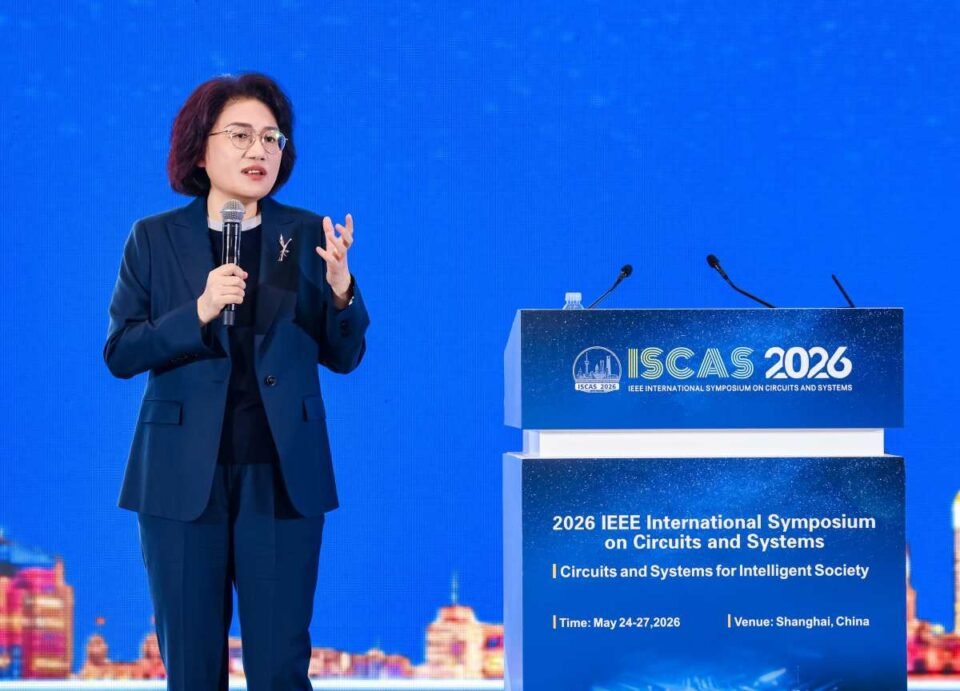
At the 2026 IEEE International Symposium on Circuits and Systems (ISCAS), HUAWEI’s He Tingbo delivered a keynote speech titled “New Semiconductor Path in Practice,” where she introduced the Tau (τ) Scaling Framework, a new principle for future semiconductor development.
The framework proposes replacing geometric scaling with time (τ) scaling as a new guiding principle for the evolution of both semiconductors and electronic systems. Based on this principle, innovative technologies such as LogicFolding can be used to continuously compress signal propagation delay and steadily improve transistor density, which will drive the ongoing evolution of semiconductors and electronic systems, says Huawei.
According to Huawei, in recent years, Moore’s Law – which has guided the semiconductor industry for more than five decades – has faced severe physical limits and diminishing economic returns. The global industry has been increasingly constrained by the slowdown in the geometric scaling of transistors and the erosion of cost-per-transistor benefits. The industry must now tackle the urgent and common challenge of overcoming the physical constraints of traditional processes and finding a new, sustainable evolution path that can match surging computing demands. This is where the Tau (τ) Scaling framework comes into play.
Shifting Focus from Physical Size to Signal Speed with Tau (τ) Scaling Framework
In technical terms, the Tau (τ) framework—informally dubbed ‘He’s Law’ by some industry peers after He Tingbo—shifts the optimization benchmark from spatial dimensions to temporal efficiency. In circuit physics, (τ) represents the RC time constant (the time required for a signal to transition between states).
Rather than chasing smaller physical transistors via advanced lithography, Huawei’s approach centers on a multi-level mechanism designed to minimize this time constant across four layers of the hardware stack:
- The Circuit Layer (LogicFolding): Moving away from traditional two-dimensional, planar circuit layouts that require long horizontal signal routing, this architecture physically stacks and “folds” critical paths vertically. Huawei claims this vertical integration significantly shortens wiring, reduces resistive and capacitive loads, and boosts effective transistor density.
- The Device Layer: Optimization centers on minimizing resistance and parasitic capacitance at the underlying physical layer of the transistors and interconnects.
- The Chip Layer: This involves full-stack coordinated design across software, silicon, and architecture to achieve fine-grained control over data flows and enhance system-level parallelism.
- The System Layer (UnifiedBus): Huawei has introduced an interconnect protocol designed to enable unified memory addressing across computing systems, aiming to reduce end-to-end communication latency.
Commercial Roadmap and the 2031 Performance Target
While presented as a long-term industry framework, He Tingbo in her keynote elaborated that the underlying principles are already operational, claiming to have designed and mass-produced 381 chips utilizing elements of the Tau framework over the past six years.
The architecture is set for its first high-profile commercial deployment in Fall 2026 with the launch of upcoming flagship Kirin mobile processors. This will be the first commercial silicon to officially feature the LogicFolding architecture.
Looking ahead, Huawei projects that by 2031, this design methodology will allow its high-end processors to achieve a transistor density equivalent to a 1.4-nanometer (nm) process node.
“We believe that openness and collaboration are key to driving ongoing progress in the semiconductor industry. No single company can independently find all the answers along the path of semiconductor evolution, says He Tingbo. “With the Tau (τ) Scaling Framework, we look forward to working closely with scientists, engineers, and industry partners around the world to drive the sustainable development of the semiconductor and electronics industries.”
